.png)
How Automation Trends Influence Hand Soldering, Rework, and Repair
The evolution of electronics and devices must keep pace to meet today’s operator challenges. As technology in the electronics industry rapidly advances, electronic devices are getting smaller, faster, and more functional. Advanced printed circuit ...
The evolution of electronics and devices must keep pace to meet today’s operator challenges. As technology in the electronics industry rapidly advances, electronic devices are getting smaller, faster, and more functional. Advanced printed circuit boards (PCBs) are now double-sided with stacked multiple layers. Thus, they are far more complex than conventional PCB designs and contain more components in tighter spaces, creating high-density interconnect (HDI) PCB configurations.
The evolution of electronics and devices must keep pace to meet today’s operator challenges. As technology in the electronics industry rapidly advances, electronic devices are getting smaller, faster, and more functional. Advanced printed circuit boards (PCBs) are now double-sided with stacked multiple layers. Thus, they are far more complex than conventional PCB designs and contain more components in tighter spaces, creating high-density interconnect (HDI) PCB configurations.
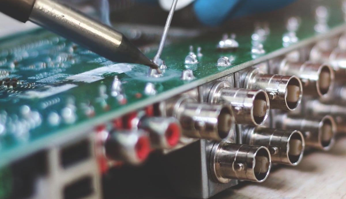
Today’s high-power industrial electronics and high-frequency telecommunication devices present additional challenging applications, which need to be completed by operators using hand soldering. These devices tend to utilize more metal in their designs for multiple reasons.
For example, multilayered copper ground planes provide signal integrity by reducing internal cross-talk interference, and large metal heat sinks dissipate heat away from heat-sensitive components. The electronics inside electric vehicle charging stations, alternating current/direct current converters, Wi-Fi, and radar are examples of highly metalized electronic assemblies. Highly metalized PCBs create a high-thermal demand (HTD) during hand soldering because the high metal content conducts heat away from the soldering tip. This HTD makes it difficult to maintain the soldering tip temperature needed to melt the solder and create a good solder joint. Technicians might compensate by extending dwell time (the time they hold the hot tip of the soldering iron to the solder joint) or by raising the temperature at the tip of the soldering iron. These compensation methods not only decrease the life of the soldering tip but also result in damage to circuit boards and heat-sensitive components

The evolution of electronics and devices must keep pace to meet today’s operator challenges. As technology in the electronics industry rapidly advances, electronic devices are getting smaller, faster, and more functional. Advanced printed circuit boards (PCBs) are now double-sided with stacked multiple layers. Thus, they are far more complex than conventional PCB designs and contain more components in tighter spaces, creating high-density interconnect (HDI) PCB configurations.
The Increasing Use of Automation
Automated assembly processes and automation equipment used in surface-mount technology (SMT) — such as pick-and-place robotics as well as wave and reflow soldering — have enabled rapid evolution in the electronics industry toward HDI PCBs and the miniaturization of components. The increasing use of automation has improved efficiencies and reduced manufacturing costs. It is also moving electronic assembly manufacturing closer to Industry 4.0, where data is fully documented, for full traceability, with lights-out manufacturing.
Despite this continuous movement, hand soldering is still necessary and still plays a key role in the manufacturing of electronic devices. Certain specialty, irregular, or heat-sensitive components must be hand soldered. With automation fulfilling the majority of electronic assembly operations, the remaining hand-soldering operations have become more challenging, requiring higher skilled soldering technicians, improved process controls, and advanced hand-soldering tools and equipment.
Although automated SMT assembly processes allow for the precise placement of components, these processes are not defect free. Issues such as bridging, tombstoning, slump, solder beading, insufficient solder, and damaged components require manual rework to repair or replace them. On high-density PCBs, components are not only exceedingly small but also extremely close together. Repairing electrical connections or removing and replacing small-scale chip packages must be done in very small spaces without damaging surrounding components. Specialized tools such as high-performance ultra-fine soldering tips, tweezers, and hand pieces are required for this type of high-precision rework, which often needs to be performed under a microscope or with the assistance of a camera to help accurately place, solder, and repair small-scale fine-pitch components.
Facing New Challenges
Today’s high-power industrial electronics and high-frequency telecommunication devices present additional challenging applications, which need to be completed by operators using hand soldering. These devices tend to utilize more metal in their designs for multiple reasons.
For example, multilayered copper ground planes provide signal integrity by reducing internal cross-talk interference, and large metal heat sinks dissipate heat away from heat-sensitive components. The electronics inside electric vehicle charging stations, alternating current/direct current converters, Wi-Fi, and radar are examples of highly metalized electronic assemblies. Highly metalized PCBs create a high-thermal demand (HTD) during hand soldering because the high metal content conducts heat away from the soldering tip. This HTD makes it difficult to maintain the soldering tip temperature needed to melt the solder and create a good solder joint. Technicians might compensate by extending dwell time (the time they hold the hot tip of the soldering iron to the solder joint) or by raising the temperature at the tip of the soldering iron. These compensation methods not only decrease the life of the soldering tip but also result in damage to circuit boards and heat-sensitive componentsFig. 1 — Thermal image of an HTD PCB showing the heat path as heat is pulled away from the solder tip.
Another method of compensating for HTD challenges associated with highly metalized PCBs is preheating the circuit board and attempting to solder while the board is hot. This creates an ergonomic safety issue for soldering technicians. Specifically, preheating the PCB increases the risk of technicians getting burned during the soldering operation. And because the components are quite small, technicians tend to get closer to the PCB to better see their work, further increasing that risk.
Innovations in the industry, developed by manufacturers of soldering equipment, are addressing these challenges. These solutions include the use of inductive heating with adjustable temperature to improve performance, inductive SmartHeat® fixed temperature systems to remove the risk associated with operators adjusting the temperature, and specialized soldering software to communicate with operators to inform when connection validation or intermetallic compound formation is complete for high-quality solder joints.
Another area that manufacturers of hand-soldering equipment need to address ties to the loss of some level of traceability during the manufacturing process when automation is not used. Operations managers must understand such things as solder joint count, good vs. bad solder processes, number of consumables used, consumable life, and differences in productivity between operators to improve productivity, throughput, and cost management. Additionally, line managers need to get alerts to ensure that operators are following correct temperature management and utilizing correct tips and geometries, systems are working correctly, and electrostatic discharge events are properly recorded.
Integrated Internet of Things data-tracking systems can document associated solder joints with specific printed circuit board assemblies (PCBAs), thus filling this traceability hole. This can only happen if proper soldering technology is utilized on the manufacturing floor.
Today, manufacturers are offering such innovations as chip-in-cartridge technology to communicate proper geometries, solder joint validation software such as Connection Validation, fixed temperature cartridges, operator lockouts, and monitoring of power curves to start this process. As gateways and application software become more available, this will allow for managers on the floor to better understand what is happening from the hand-soldering processes.
With the evolution of electronic devices and their assembly methods, hand-soldering tools, equipment, and processes must keep pace to meet the daily challenges faced by today’s operators.